AI Chip Substrates: When to Switch to Glass
AI chip substrates are performance-critical components that carry signals and power between chiplets and HBM. This guide explains the distinct roles and commercialization requirements of FC-BGA, multilayer PCBs, MLCC, and glass substrates.
- FC-BGA is a package substrate that connects chips to the system board.
- Multilayer PCBs connect multiple packages and components at the system level.
- Glass substrates offer flatness and dimensional stability, but yield and processability remain challenges.
- CPO can be implemented without glass substrates, so the adoption timelines for the two technologies may differ.
- Investment decisions should distinguish among development announcements, customer certification, mass production, and revenue.
AI semiconductor substrates are performance-critical components that connect chiplets and HBM while distributing power and signals. FC-BGA and high-layer-count PCBs are already in use, but glass substrates still require validation for mass production. Investment decisions should distinguish technical feasibility from actual revenue.
Technical reference: Intel Newsroom’s announcement on glass substrates; verify the announcement date and subsequent schedules in each company’s latest disclosures
The Role of Substrates in AI Semiconductors
A substrate provides an electrical interconnection network in addition to serving as a board that secures chips. Signal paths and power networks are also formed within the substrate. Package size and wiring density affect system performance.
AI accelerators do not consist solely of GPUs or dedicated computing chips. HBM and input/output chiplets are also connected over short distances. Heterogeneous integration combines chips made with different processes into a single package.
Chiplets are an approach that divides a large monolithic chip into multiple functional blocks. Not all chiplets automatically improve cost or yield. Interface and packaging costs must also be included in the calculation.
Substrates perform the following functions.
- High-speed signal connections between chips
- Stable distribution of power and ground
- Support for heat-transfer paths from chips
- Connection of terminals with different sizes and pitches
- Mechanical attachment of the package to the system board
The Precise Distinction Between FC-BGA and ABF
FC-BGA is a package structure widely used for high-performance chips. The chip is connected face-down to the substrate through bumps. Solder balls beneath the substrate connect it to the system board.
ABF does not mean FC-BGA itself. ABF is a family of build-up insulating materials used in fine wiring layers. Therefore, using FC-BGA and ABF substrate as synonyms in every context is inaccurate.
AI packages may require large areas and many input/output connections. Manufacturing becomes more difficult as the number of layers and wiring density increase. However, whether shortages exist varies by period and specification.
Comparison of High-Layer-Count PCBs and Package Substrates
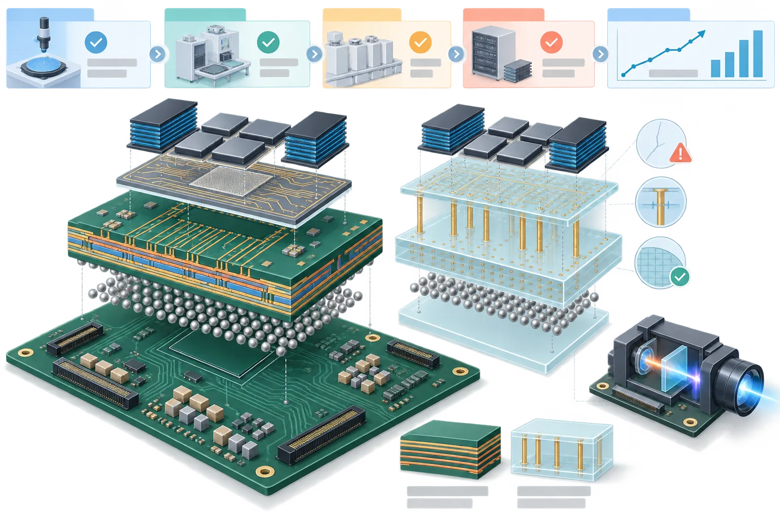
The two types of substrates differ in mounting location and wiring precision. FC-BGA is placed directly beneath the semiconductor die. High-layer-count PCBs connect multiple packages and components at the system level.
| Category | FC-BGA Package Substrate | High-Layer-Count PCB·MLB | Glass-Core Substrate·Interposer |
|---|---|---|---|
| Primary location | Between the semiconductor die and system board | Main board in servers and networking equipment | Inside the package or in an intermediate interconnection layer |
| Primary role | Fine-pitch conversion and signal·power connections | System-level connection of packages and connectors | Large-area fine wiring and dimensional stability |
| Key challenges | Fine wiring, warpage, yield | Interlayer alignment, signal loss, drilling | Breakage, through-glass vias, metal adhesion, yield |
| Market stage | Commercial mass production | Commercial mass production | Development·trial production·customer qualification coexist |
| Metrics to verify | Product specifications and utilization rate | Share of revenue from high-layer-count products and customer qualification | Pilot yield and acquisition of mass-production customers |
MLB is a broad term referring to multilayer printed circuit boards. Not every MLB is a high-value-added product for AI servers. It is also difficult to assess product complexity and profitability based solely on the number of layers.
For high-speed signals, materials and stack-up structures work together. Insertion loss and impedance control must also be examined. Connectors and via structures also affect overall performance.
The Relationship Between MLCC and Substrates
MLCC is not a substrate but a passive electronic component. It stores electrical charge to mitigate sudden voltage fluctuations. Around processors, it is used for decoupling and noise suppression.
As AI accelerators consume more power, power-network design becomes more difficult. The required number and specifications of MLCCs vary by product. Demand volume cannot be calculated uniformly based only on improvements in chip performance.
When assessing potential benefits for MLCC suppliers, the product mix matters more than unit count. Rated voltage and capacitance affect unit prices. Size and temperature characteristics also determine actual adoption.
Why Glass Substrates Are Drawing Attention
Glass may offer advantages in flatness and dimensional stability. Its coefficient of thermal expansion can also be adjusted depending on composition and design. These properties are advantageous for reducing alignment errors in large packages.
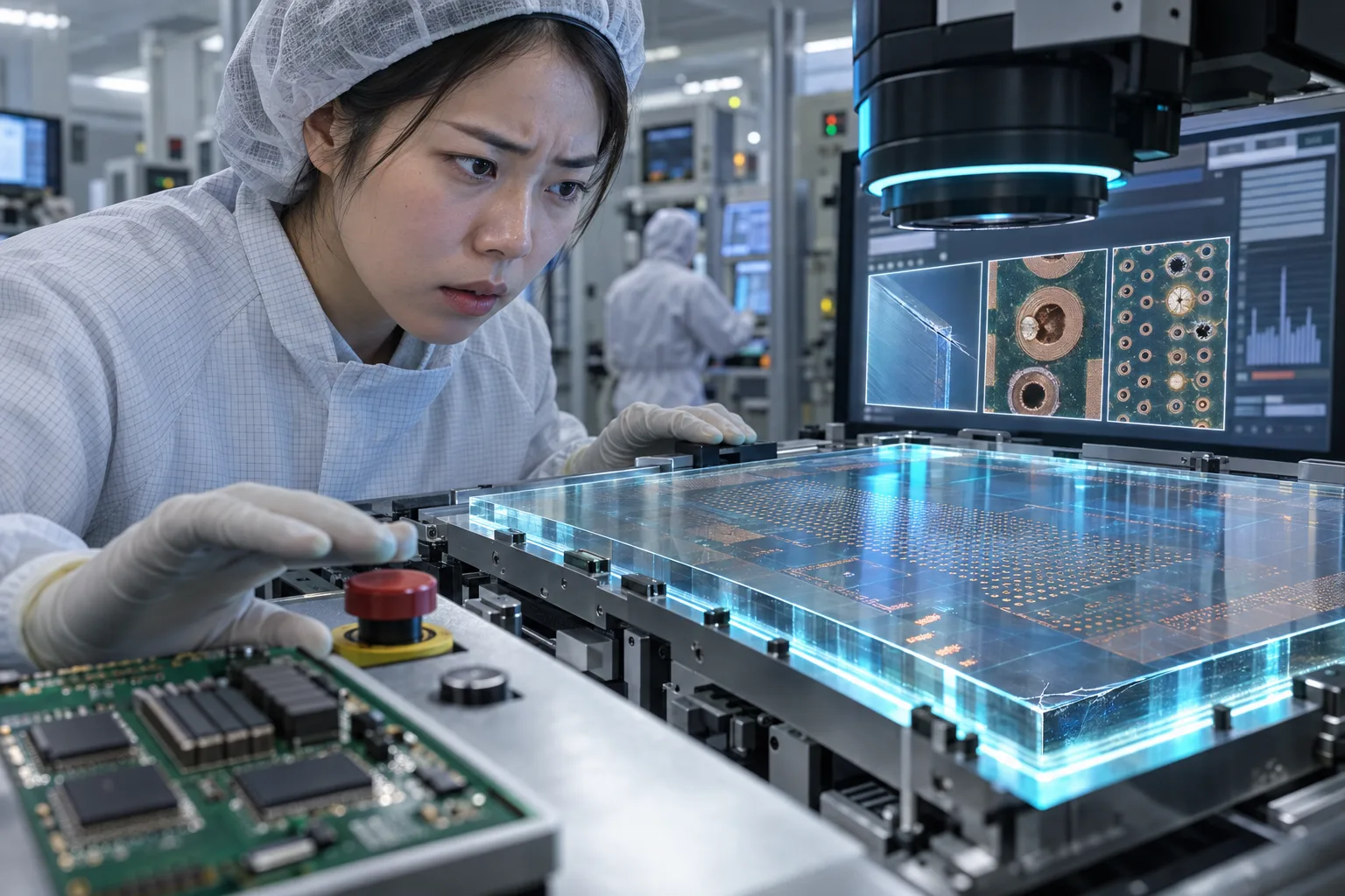
Glass cores may require through-glass vias. Laser processing and metal-filling processes are used. Microcracks and metal adhesion affect yield.
Glass does not always provide better heat dissipation than plastic. Thermal performance depends on the material’s thermal conductivity and the overall package structure. Actual cooling is evaluated by including heat sinks and cooling systems.
Intel announced glass substrate technology for next-generation advanced packaging, and the announcement date can be verified in Intel Newsroom’s official announcement. This does not mean an immediate industry-wide transition to mass production. Customer qualification and adoption timelines for each company should be verified in the latest disclosures.
Conditions Linking Glass Substrates and Optical Communications
Glass substrates and CPO may be related, but the relationship is not essential. CPO is a technology that places optical engines close to switch chips. Its purpose is to reduce the distance and power issues of copper interconnections.
The mere fact that glass is transparent does not reduce optical loss. The material and geometry of the optical waveguide determine signal loss. Coupling structures and wavelength characteristics must also be designed separately.
CPO can also be implemented with silicon photonics and organic substrates. Glass substrates are one potential future integration option. Treating the commercialization schedules of the two technologies as one leads to errors.
Substrate Selection by Requirement
Substrate selection varies depending on package size and input/output density. No single material will replace every AI system. Cost and existing production facilities are also adoption criteria.
| Required condition | Technology considered first | Rationale |
|---|---|---|
| High-performance processor packaging | FC-BGA | Suitable for fine wiring and input/output connections |
| System-level connection of multiple packages | High-layer-count PCB | Handles board-level interconnections and power distribution |
| Ultra-fine connections between chiplets | Silicon interposer or high-density bridge | Enables short, dense wiring |
| Dimensional stability in large packages | Consider glass-core substrates | Can utilize flatness and thermal expansion properties |
| Integration of short-range optical input/output | CPO and optical waveguide technology | Can reduce electrical interconnection distances |
| Suppression of voltage fluctuations | MLCC and power-management circuits | Provide instantaneous current and mitigate noise |
Example of Signal-Path Calculation
Package performance can be assessed by dividing it into the entire signal path. For example, multiple interconnection segments exist between a GPU and HBM. Improving only one segment may leave the overall bottleneck unresolved.
- Check the bump connections between the GPU and HBM.
- Check the wiring structure of the interposer or bridge.
- Distinguish the signal layers from the power layers in the package substrate.
- Check the connections between the solder balls and high-layer-count PCB.
- Add up losses through the connectors and network optical modules.
No common fixed values can be applied to this example. This is because wiring lengths and data rates differ by product. Calculations require the vendor’s design rules and measurement results.
Common Mistakes and Misconceptions
A frequent mistake is treating technological direction and investment performance as the same thing. Profitability may deteriorate even as technology adoption increases. In the early stages, depreciation and low yields raise costs.
- Treating FC-BGA and ABF as complete synonyms.
- Interpreting every MLB as being for AI servers.
- Assuming the number of MLCCs installed is the same in every AI accelerator.
- Assuming glass always has better heat-dissipation performance than organic materials.
- Concluding that optical communications will adopt glass based solely on its transparency.
- Interpreting a development announcement as customer qualification or mass-production revenue.
- Failing to verify the survey date and scope of market-share figures.
A specific company’s market share may vary by research firm. Classification criteria for AI server applications are also not standardized. Figures without sources and reference years are difficult to use as an investment basis.
Metrics for Verifying Companies and Industries
Companies involved in glass substrates should be evaluated by production stage. Research and development and pilot production differ from mass production. Mass-production facilities also do not guarantee customer revenue.
| Verification stage | Facts to verify | Documents to check |
|---|---|---|
| Technology development | Sample production and process scope | Official technology announcements, patents |
| Trial production | Pilot-line installation and operation | Annual reports, facility disclosures |
| Customer qualification | Customers conducting evaluations and qualification stage | Earnings releases, official contract disclosures |
| Mass production | Production capacity and yield stabilization | Quarterly reports, investor-relations materials |
| Revenue recognition | Revenue and profit from the relevant business | Audit reports, business-unit results |
Some contracts do not disclose customer names. In such cases, revenue growth and utilization rates should be checked together. Orders may not follow even if capital expenditures increase.
Verification Sequence for Semiconductor Substrate Investments
Investment reviews should begin with disclosures rather than technical descriptions. A company’s actual exposure must be verified to distinguish a theme from business performance. Materials can be cross-checked in the following order.
- Find the share of revenue generated by the substrate business in the annual report.
- Check whether FC-BGA revenue is separated from general PCB revenue.
- Verify the target products and operating schedule for capital investments.
- Determine whether customer qualification is in the development, testing, or mass-production stage.
- Examine how utilization rates and depreciation expenses affect profitability.
- Check customer concentration and inventory changes together.
- Cross-check market share against the research firm and reference year.
Samsung Electro-Mechanics and Japanese substrate companies have different business portfolios. It is difficult to compare corporate value based solely on market share. The profit contributions of MLCCs and package substrates must also be separated.
The same standards are required for glass substrate companies. Possessing pilot facilities alone is insufficient to conclude that a company has a commercial advantage. Verify whether yields and customer qualification status are disclosed.
Where to Find Official Technical Documents
Official technical descriptions of glass substrates can be found in Intel Newsroom’s official announcement. The TSMC 3DFabric technology page covers chiplet and interposer structures. Information on CPO and silicon photonics is available on NVIDIA’s technology pages.
Investment amounts and mass-production schedules for each company may continue to change. The company’s annual reports and stock-exchange disclosures should be checked first. Brokerage forecasts should be read separately from the company’s confirmed contracts.
FAQ
Do FC-BGA and ABF substrate mean the same thing?
They do not mean exactly the same thing. FC-BGA is a package structure that uses flip-chip technology and solder balls, while ABF is a family of insulating materials primarily used for the substrate's fine wiring layers.
How do high-layer-count PCBs differ from semiconductor package substrates?
A package substrate converts fine pitches directly beneath the semiconductor die. A high-layer-count PCB connects multiple components, such as packages, memory, and connectors, at the system level.
Will glass substrates replace all conventional organic substrates?
It has not been confirmed that they will fully replace them. Glass offers advantages in flatness and dimensional stability, but challenges remain in breakage, through-glass via fabrication, metal adhesion, cost, and yield.
Do glass substrates have better heat dissipation performance?
Not always. Heat dissipation must be evaluated based on the entire structure, including the die, adhesive layer, heat sink, and cooling system, rather than solely on the material's thermal conductivity.
Is a glass substrate essential for implementing CPO?
It is not a requirement. CPO can also be implemented using silicon photonics and conventional packaging technologies, while glass substrates are an option that could be used to integrate optical waveguides in the future.
Do AI accelerators always contain thousands of MLCCs?
The quantity varies by product, so a fixed number cannot be applied. The required quantity and specifications vary depending on the power architecture, package size, capacitance, and placement method.
How can the mass-production potential of a glass substrate company be assessed?
The pilot line, customer qualification, production capacity, yield, utilization rate, and revenue contribution must be assessed at each stage. Mass-production revenue should not be assumed based solely on a development announcement or equipment installation.
Is the shortage of FC-BGA supply an ongoing structural phenomenon?
It cannot be assumed to persist across all specifications. Supply conditions vary depending on package size, wiring complexity, customer qualification, the timing of capacity expansion, and end demand.
Sources
Images