Injoys
The competitive criteria for AI semiconductors are expanding beyond simple computation counts to how much data can be stored and moved using little power. In large-scale AI inference, GPUs may sit idle not because they cannot perform computations, but because they do not receive the required model weights and KV cache in time.
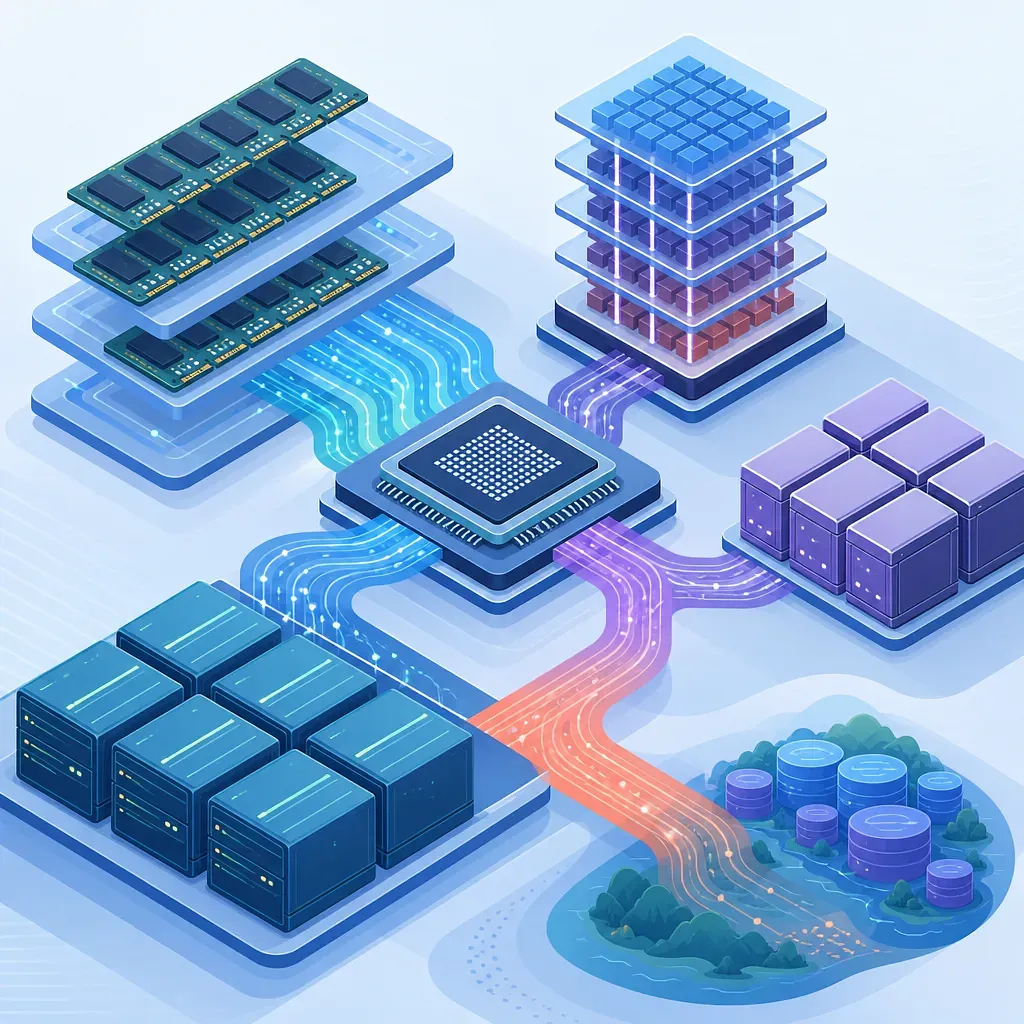
This change is often described as a “shift from GPU-centric to memory-centric computing.” However, this does not mean that GPUs are disappearing or have stopped advancing. More precisely, it is a move toward jointly designing GPUs, HBM, external memory, storage, networking, and software as a single data movement system.
What Is Memory-Centric Computing?
Memory-centric computing is an approach that takes memory location, bandwidth, capacity, and computing capabilities as the starting point of system design to reduce the cost of repeatedly moving data to processors.
The arithmetic throughput of AI chips has increased rapidly, but retrieving data from outside the chip remains relatively slow and consumes significant power. As a result, the following technologies are becoming important together.
- HBM placed close to a GPU or AI accelerator
- 3D packaging that vertically connects memory and logic
- Customized HBM that incorporates control or limited computing functions into the base die
- Memory expansion and pooling using CXL
- The HBF concept, which connects NAND flash through a wide interface
- Optical interconnects intended to reduce transmission power between chips and servers
- PIM and near-memory computing, which process data close to memory
In other words, memory-centric computing does not refer to a single memory product. It is a system principle that combines multiple tiers, from fast memory to high-capacity storage, to minimize data movement.
Why AI Inference Intensifies the Memory Bottleneck
Model Weights and the KV Cache Create Different Burdens
The memory required for AI inference can broadly be divided into model weights, activations generated during execution, and the KV cache. Model weights occupy a fixed amount of space even when there are no requests, while the KV cache grows according to input length, output length, and the number of concurrent requests.
To avoid recomputing previous tokens from scratch each time, transformer models store attention key and value information for each layer in the KV cache. In simplified terms, the KV cache size for a single request is proportional to the following factors.
The exact KV cache size must be verified from the model architecture and implementation specifications.
The KV cache stores keys and values separately. Therefore, as context grows longer or more users are processed simultaneously, the KV cache grows rapidly. Not every model uses millions of tokens, nor does cache size uniformly increase by hundreds of times, but it is clear that long-context inference and agentic tasks increase memory pressure.
Hallucinations and Memory Capacity Are Not the Same Problem
Longer context and retrieval-augmented generation can provide models with more supporting evidence. However, increasing memory alone does not eliminate hallucinations. The quality of search results, prompt design, the model’s reasoning capabilities, source verification, and evaluation frameworks are also necessary.
Software Can Reduce Physical Memory Demand
The KV cache bottleneck is not solved solely by adding hardware.
- MQA and GQA reduce the number of KV heads that must be stored.
- Quantization reduces the number of bytes used by weights and caches.
- PagedAttention manages caches in pages, mitigating fragmentation and waste.
- Continuous batching efficiently groups multiple requests.
- Prefix caching reuses repeated system prompts or shared context.
- Cache eviction and tiered offloading move less important information to slower memory.
Therefore, the actual amount of memory investment in a data center depends not only on model size but also on the efficiency of the inference engine.
The Memory Hierarchy of AI Data Centers
It is difficult for a single type of memory to satisfy speed, capacity, cost, and power efficiency requirements all at once. AI data centers are likely to evolve into the following hierarchy.
| Tier | Representative Technologies | Strengths | Main Limitations | Expected Role |
|---|---|---|---|---|
| On-chip | SRAM, registers | Shortest latency | Very limited capacity and high area cost | Immediately needed data and intermediate computation results |
| Adjacent to accelerator | HBM | High bandwidth and relatively short latency | Capacity, packaging cost, and thermal constraints | Active weights and frequently used KV cache |
| Server memory | DDR, CXL-connected memory | Greater expandable capacity than HBM | Farther from accelerators and lower bandwidth | Cache expansion, model tiering, and memory pools |
| High-bandwidth flash | HBF concept | High NAND-based density and non-volatility | Read latency, write endurance, and control complexity | Less frequently used weights and KV cache tiers |
| Storage | NVMe SSD | High capacity and low cost per bit | Longer latency than memory | Checkpoints, datasets, and cold data |
The key is not for either HBM or HBF to win, but to deploy multiple tiers according to how frequently data is used.
The Next-Generation Memory Competition Revealed by FMS 2026
FMS, held in Santa Clara, United States, in August 2026, addressed post-HBM AI memory and storage architectures as major agenda items. Discussions centered on taller stacks, high-capacity NAND-based tiers, customized memory, and data center connectivity technologies.
Samsung Electronics’ GHBM and the HBF discussed by SK hynix with Google and SanDisk were introduced as examples illustrating this direction. However, it is difficult to conclude that names such as GHBM, HBF, and THBM are all universal generation names finalized under identical JEDEC specifications. Technologies at the corporate announcement stage, joint development concepts, and standardized commercial products must be distinguished from one another.
Moreover, a higher generation name does not necessarily make actual AI services faster. Effective bandwidth, memory capacity, latency, power, cooling, package yield, and software support must all be compared together.
HBM’s Strengths and Capacity Limitations
HBM vertically stacks multiple DRAM dies and connects them using through-silicon vias and a wide interface. Its key advantage is that it can supply large amounts of data in parallel close to the accelerator, unlike conventional board-level memory.
However, HBM capacity cannot be increased indefinitely.
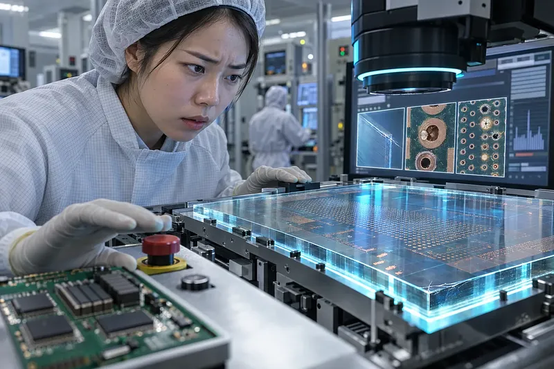
- As the number of stacked layers increases, manufacturing yield and testing become more difficult.
- The package area required to place the GPU and HBM together increases.
- Heat generated by the accelerator and memory must be removed from a confined space.
- Power delivery networks and interposer wiring also become more complex.
- Using expensive HBM to store even infrequently accessed data reduces economic efficiency.
For this reason, tiering is becoming important, with HBM handling the most frequently used data and the rest being moved to CXL memory, flash, or SSDs.
Can HBF Replace HBM?
HBF stands for High Bandwidth Flash and is a concept that parallelizes and stacks NAND flash to create a high-bandwidth memory tier closer to accelerators than conventional SSDs. Because NAND offers higher density and non-volatility than DRAM, it has the potential to store more data in the same physical space.
However, NAND has different characteristics from DRAM.
- It has longer read latency.
- Data must be erased before it can be overwritten.
- Endurance must be managed according to the number of writes.
- Bad blocks, error correction, and wear leveling must be handled.
- It is better suited to large sequential accesses than small, irregular accesses.
Therefore, even if HBF is commercialized, it is more likely to function as a high-capacity tier between HBM and SSDs than to directly replace HBM. Read-heavy model weights, infrequently reused caches, checkpoints, and retrieval data could be candidates. Its actual suitability will depend on interface standards, latency, endurance, controllers, and inference software support.
The 3D Packaging Challenges Raised by GHBM and THBM
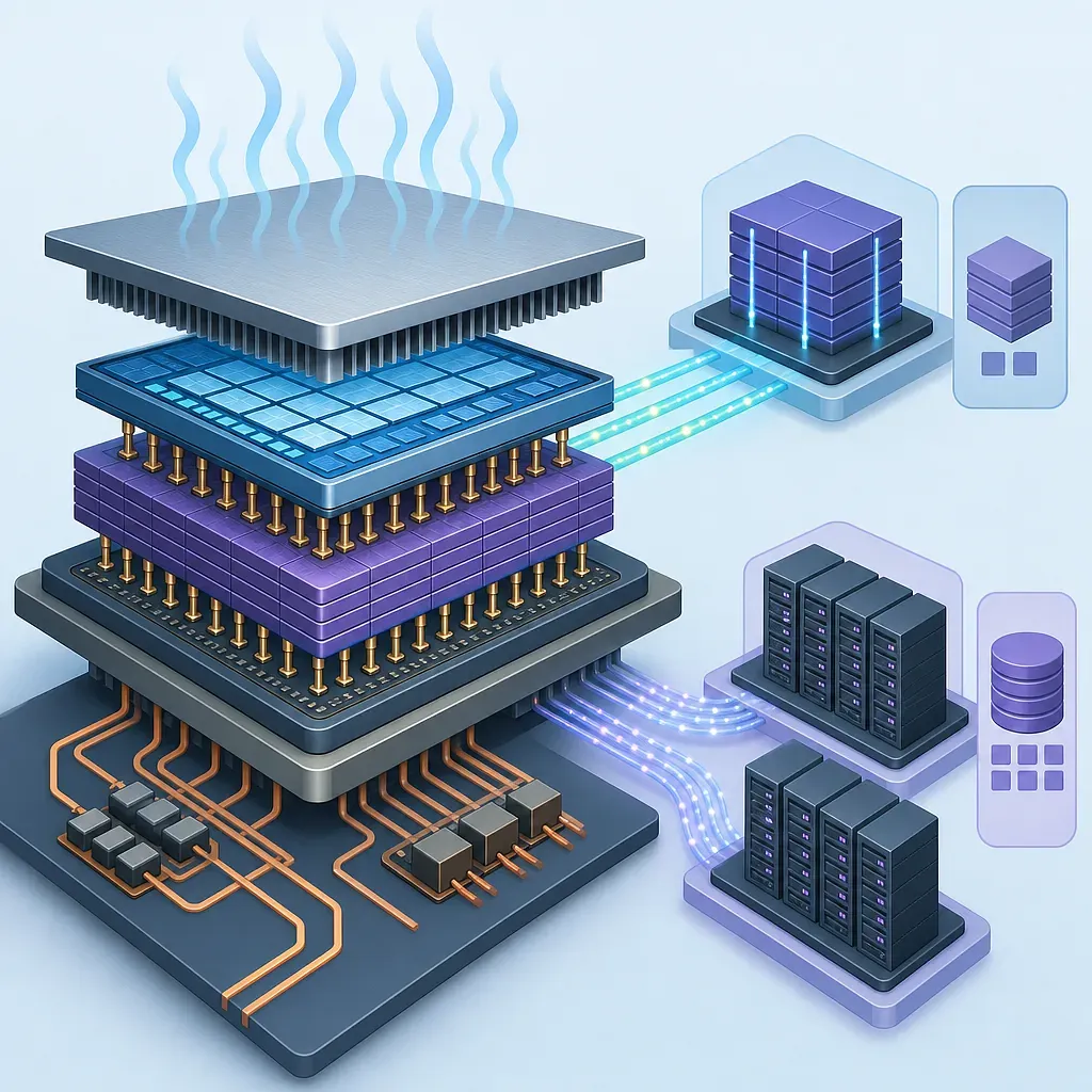
Placing accelerators and HBM side by side within a package imposes limits on connection width and package area. To overcome these limitations, concepts have emerged that vertically stack logic and memory to shorten wiring distances.
A Structure That Places Memory Above the GPU
The concept introduced as GHBM or Z-axis HBM aims to reduce data movement distances by vertically integrating the GPU and HBM. Numerous short vertical connections are expected to provide high bandwidth and low I/O power.
The problem is heat. When memory is placed above the GPU, heat generated by the GPU may pass through the memory on its way to the cooling device. The expression “the memory melts” is closer to a metaphor emphasizing the thermal problem than a technical explanation. The actual risks are exceeding the allowable temperatures of the bonding interfaces and memory, increased leakage current, performance throttling, and reduced lifespan.
Memory Below, GPU Above
THBM, reportedly proposed by Professor Kim Jung-ho’s team at KAIST, is based on the idea of placing the GPU above the HBM stack so that the heat-generating logic sits closer to the cooling device. This may be advantageous for heat dissipation, but the following challenges remain.
- Mechanical stability of the heavy logic die and memory stack
- Power delivery and signal routing
- Bonding yield for dies manufactured using different processes
- The ability to replace and test defective dies
- Package design that includes the cooling plate
The competitiveness of vertical stacking cannot be determined from a conceptual diagram alone. Measurements of thermal resistance, effective bandwidth, yield, and total cost of ownership are required.